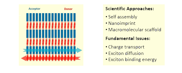
Directed Assembly
The morphology and microstructure of an organic thin film have significant impacts on the optical/electronic properties and device characteristics. For instance, single©\crystalline organic films exhibit much higher charge carrier mobility than their amorphous and polycrystalline counterparts. While producing highly ordered organic molecular assemblies is not trivial and all single crystalline organic semiconductors developed so far suffer from very limited size of nanometers or micrometers. In most of cases, the grain boundaries with disorder structures in polycrystalline thin films dominate device performance. Therefore, it is of great interest to develop practical approaches to achieving large area defects-free organic thin films. In addition, molecular assemblies with long-range order structures provide a perfect platform for the study of their intrinsic physical properties. Our efforts focus on self-assembly and directed-assembly of organic electronic materials. Post-treatments on organic thin films have dramatic effects on the film morphology, which often introduce molecular reorganization leading to significant enhancement of charge carrier mobility. These methods include thermal annealing, solvent annealing, solvent-vapor exposure, etc. Our research attempted to explore new methods to turn disordered molecular assemblies into highly ordered organic thin films with enhanced electronic properties. Our recent studies have shown that thermal nanoimprinting of a solution processed amorphous film of small molecule could generate stable nanoscale patterns with highly ordered molecular stacking inside the domains. More recent work has shown large area phase change from amorphous to crystalline morphology for these solution processed small molecule films via thermal imprint with flat mold. Our work certainly opens a new avenue for the facile control of molecular assembly in the solid state.
Research efforts in achieving long range ordered organic semiconducting thin films, with high charge carrier conductivity and photoconductivity, would be continued. Several approaches will be explored, including:
- Synthetic control of molecular geometry and shape
- Macromolecular scaffolds assisted assembly of small molecules
- External forces induced reorganization of random molecular assemblies
Molecules with geometry and shape in favor of intermolecular packing will be developed to obtain one-dimensional long-range order nanostructures. Besides synthetic control of molecular structure, applying external environment regulation is another powerful approach to achieving highly ordered molecular architectures. Two macromolecular scaffoldings will be applied to direct the assembly of organic semiconductors, including peptoids for two-dimensional organic sheets and dendronized polymers for one-dimensional organic semiconducting nano-objects. Applying external forces, such as thermal imprint and laser annealing, represents another interesting approach to turn disordered molecular assemblies to highly ordered ones with enhanced properties.