The Nienhaus Lab @ FSU Research
Overview: Disentangling the Optoelectronic Properties of Semiconductors
Research in the Nienhaus lab will aim to understand the detailed optoelectronic properties of semiconductors at the nanoscale, and their interactions in the ensemble. We hope to advance tip-enhanced microscopy beyond the current capabilities to probe the cause of reduced efficiencies in optoelectronic devices made of emerging (nano-)materials. Research directions will focus on synthesis of semiconductor materials such as quantum dots and perovskites, optical spectroscopy and the combination of optical spectroscopy and scanning probe microscopy.
Solid-State Infrared-to-Visible Upconversion Sensitized by Lead Halide Perovksite Thin Films
Efficient photon upconversion holds the potential for the improvement of emerging technology and breakthroughs in many areas, including solar energy and infrared sensing. Current triplet-triplet annihilation upconversion systems rely on metal-organic complexes and quantum dots as sensitizers but struggle with low achievable efficiencies. Bulk semiconductor materials like perovksites are explored as an alternative sensitizers that could eliminate problems created by the existing quantum confined sensitizaters.
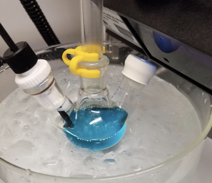
Synthesis of New Glowy Things
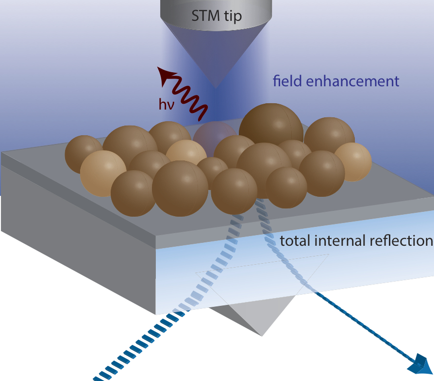
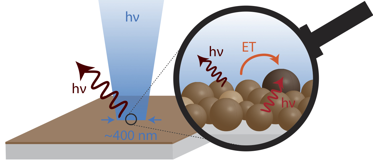
Scanning Tunneling Microscopy